We have reviewed with you all the main radio components, their principle of operation and their use in various devices and systems.
I hope it was interesting and useful for you.
Автор: radiotechnician
LED
Light emitting diode is a semiconductor device that converts an electric current directly into light.

The luminescence occurs during the recombination of electrons and holes in the region of the pn junction. For luminescence, the band gap in the active region of the LED must be close to the energy of light quanta in the visible range
Of the advantages should be highlighted: electrical current is converted directly to light,
the LED emits in a narrow part of the spectrum, its color is clear, the LED is mechanically durable and extremely reliable, the LED is a low-voltage appliance, and therefore safe.
In radio engineering, LEDs are used in display devices, both individually and as part of such complex structures as LED screens.
Sources:
https://en.wikipedia.org/wiki/Light-emitting_diode
https://www.toppr.com/bytes/principles-of-led/
Transformer
Transformers are designed to change the voltage of the alternating current, the coordination of electrical circuits.
The transformer in most cases consists of a closed magnetic circuit (core) with windings located on it. The number of windings can be arbitrary. One of them is connected to the source of the EMF variable and is called primary. All other windings are called secondary.
Alternating current, flowing through the turns of the primary winding, induces an alternating magnetic field in it and the core. This magnetic field intersects the turns of the secondary windings and induces (induces) EMF variables in them. The magnitude of the induced EMF of the secondary windings is directly proportional to the number of turns in these windings. Therefore, the main parameter of the transformer is the transformation ratio n: n=W1/W2 or n=U2/U1 where W1 and U1 — the number of turns and the voltage of the primary winding, W2 and U2 — the number of turns and voltage of the secondary winding.
If there are more turns in the secondary winding than in the primary winding, the alternating voltage of the secondary winding will be greater than the alternating voltage of the primary winding. Such transformers are called step-up, but on the contrary — step-down.
Sources:
http://www.cromptonusa.com/Potential%20Transformers.pdf
https://www.explainthatstuff.com/transformers.html
Zener diode
This is a special diode operating in the steady-state mode of breakdown under conditions of reverse bias of the p – n junction.

The Zener Diode is used in its “reverse bias” or reverse breakdown mode, i.e. the diodes anode connects to the negative supply.
When a breakdown occurs, the current through the Zener diode rises sharply, and the voltage at the Zener diode is maintained with a given accuracy in a wide range of reverse currents
Zener diodes are widely used as independent stabilizing elements, as well as sources of reference voltages (reference voltages) in transistor stabilizers.
Sources:
https://www.electronics-tutorials.ws/diode/diode_7.html
https://en.wikipedia.org/wiki/Zener_diode
MOSFET
Metal-oxide-semiconductor field-effect transistor is an insulated-gate field-effect transistor , which is a section of a thin layered dielectric (usually SiO2).

It is mainly used as a signal amplifier, or as a rectifier, to reduce the voltage to the desired value.
It has 4 electrodes: source, drain, substrate and gate. Under the influence of a certain current (field), the semiconductor begins to conduct electricity (amplified signal from the source to the drain). This process is controlled by a gate, to which a different current is supplied, for smooth regulation of the amplified signal. A certain current comes to the source, the shutter allows some amount to go to the drain.
The source signal of low power supplied to the gate, in this case, serves as the gate kapellmeister.
Sources:
https://www.quora.com/Whats-the-difference-between-JFET-and-MOSFET
https://electronicsforu.com/resources/learn-electronics/mosfet-basics-working-applications
https://www.youtube.com/watch?v=GrvvkYTW_0k
Junction field-effect transistor
JFET is an active semiconductor devices in which the output current is controlled by an electric field.
The three contacts of field-effect transistors are called the source (source of current carriers), the gate (control electrode), and drain (the electrode where the carriers flow).

The analogy can be drawn: the pn junction is a dam blocking the flow of charge carriers from the source to the drain. By increasing or decreasing the reverse voltage on it, we open / close gateways on it, adjusting the output current.
Advantages of field-effect transistors compared to bipolar:
high speed (due to the absence of accumulation and resorption of minority carriers);
high temperature stability;
low noise level, since the field-effect transistors do not use the phenomenon of injection of minor charge carriers;
low power consumption.
Sources:
https://www.electronics-tutorials.ws/transistor/tran_5.html
https://habr.com/ru/post/133493/
https://en.wikipedia.org/wiki/Field-effect_transistor
Bipolar transistor
The transistor is an electronic semiconductor device in which the current in the circuit of two electrodes is controlled by a third electrode.
Transistors are the reason why we know the present world as it is. Transistors came to replace electronic tubes that consumed a lot of power and were cumbersome.
The main field of application of any transistors is the amplification of a weak signal due to an additional power source. They are also used in logical gates when computing in digital technology

The bipolar transistor is of 2 types: pnp and npn.
Any bipolar transistor has 3 outputs: a collector and an emitter, between which a controlled current flows and a base — a control output
By changing the current in the base-emitter circuit, we can control the output current of the collector. Moreover, a slight change in the base current causes a significant change in the collector current.
Nowadays, transistors have reached the size of several nanometers, which has significantly increased the computing power of computers.
Sources:
https://www.youtube.com/watch?v=OwS9aTE2Go4
https://habr.com/ru/post/133136/
https://electroandi.ru/elektronika/printsip-raboty-bipolyarnogo-tranzistora.html
P–n junction
P-n junction underlies all semiconductor devices.
It occurs on the border of 2 semiconductors of different types of conductivities, n-type and p-type.
n-type — electronic conductivity.
p-type — hole conduction (hole is the lack of an electron at a position where one could exist in an atom or atomic lattice).

The main property of the pn junction is that it passes current only in one direction.
As a result of diffusion, some holes from the p-type region will transfer to the n-type region, and free electrons to the p-type region
In a thin layer of the p – n junction, electrons and holes recombine, and they form a depleted layer of the p – n junction, which is the barrier layer for the main charge carriers.
Visual representation of n-junction:
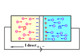
p-n junction when direct voltage is applied

p-n junction when reverse voltage is applied
Sources:
https://en.wikipedia.org/wiki/P%E2%80%93n_junction
http://radio-samodel.ru/p-n%20perexod.html
https://en.wikipedia.org/wiki/Electron_hole
Vacuum tube
It is a vacuum electronic device that works by controlling the intensity of the flow of electrons moving in a vacuum or rarefied gas between the electrodes.Currently, almost completely replaced by semiconductor devices.

Their principle of operation is based on the phenomenon of thermionic emission (emission of electrons by a heated solid body) and the effect of an electric field on moving charges.
Under the influence of the potential difference between the anode (+) and the cathode (-), the electrons reach the anode and form the anode current in the external circuit.
With the help of additional electrodes (grids), the electron flow is controlled by applying electric potential to these electrodes.
The first electronic lamp — a diode — was invented by D. Fleming (England) in 1904,
which opened the age of electronics.
The main elements of the diode are the cathode and the anode. In the diode, the current flows only in one direction — from the cathode to the anode.
Current applications:
Due to the principle of operation, electron tubes are devices that are much more resistant to such damaging factors as the electromagnetic pulse.
Vacuum tube equipment can be designed for a larger temperature and radiation range of conditions than semiconductor.
Vacuum tubes are still used in sound engineering, both amateur and professional. Designing tube sound engineering devices is one of the directions of the modern amateur radio movement.
Capacitor
A capacitor is a bipolar device that can accumulate and quickly release an accumulated electrical charge.
An interesting property of capacitors is that they do not pass direct current, because there is no direct contact between the plates, but they pass alternating current due to the electric field between the plates.

In the process of obtaining a charge of electric current, electrons (particles with a negative charge) are collected on one plate, and holes (quasi-particles, carriers of a positive charge) on the other. The separator between the positively and negatively charged particles is a dielectric, which can be used in a variety of materials.
Сapacitors are used in almost all radio engineering and various electronic circuits.
For example, they are used
• in the filters we’ll talk about later
• for smoothing pulsations when rectifying current
• in flashlights and lasers because of the possibility of creating a powerful pulse
